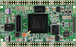
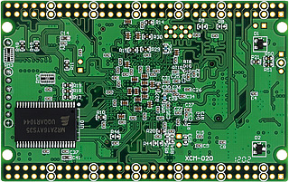
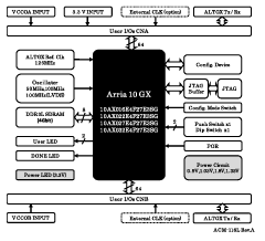
FPGA overview XC7S50 XC7S75 XC7S100 Logic Cell 52,160 76,800 102,400 Slice 8,150 12,000 16,000 Max Distributed RAM (kb) 600 832 1,100 Max Block RAM (kb) 2,700 3,240 4,320 DSP Slice 120 140 160 CMT (MMCMx1+PLLx1) Five 8 8 Max user I/O (Device) 250 338 338 Max user I/O (Board) 100 100 100 Please refer to the page of XILINX Spartan-7 for the details of FPGA outline .
- Equipped with XILINX Spartan-7 FPGA XC7S50-1FGGA484C, XC7S75-1FGGA484C or XC7S100-1FGGA484C
- 5V single power supply operation Built-in power
supply circuit required inside
Power supply sequencer installed (at the time of turning on ) - Abundant I/O externally drawn (100)
- Equipped with 5V level converter in I/O block
Controllable every 8 bits (4 bits in part) - On-board clock
50MHz (LVTTL) - Configuration ROM
Quad SPI ROM: MT25QL128ABA1ESE-0SIT (Micron, 128Mbit)
FPGA with 7-pin JTAG connector configuration
ISP
JTAG Buffer circuit to configuration ROM realizes stable download- General-purpose LED x4
- Push button switch x1
- DIP switch x1bit
- Reset function for configuration
- 6-layer board adopted
- Board size: 54mm x 86mm Credit card size
- RoHS compliant


