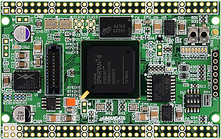
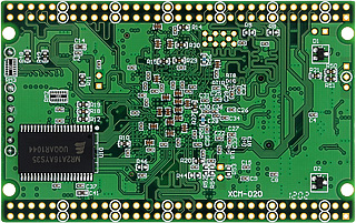
It can be used for evaluation and prototyping of Arria II GX.
FPGA overview EP2AGX45 EP2AGX65 EP2AGX95 EP2AGX125 ALMs 18,050 25,300 37,470 49,640 Logic Elements 42,959 60,214 89,178 118,143 Total memory (Kbits) 3,435 5,246 6,679 8,121 Number of multipliers (18 x 18) 232 312 448 576 Number of PLL Four Four 6 6 Maximum number of transceivers (Device) 8 8 12 12 Maximum transceivers ( Board ) Four Four Four Four Maximum number of user I/O (Device) 364 364 452 452 Maximum user I/Os ( Board ) 100 100 100 100 Please see the page of Arria II GX of ALTERA for details of FPGA outline .
- Equipped with EP2AGX45DF25C6N, EP2AGX65DF25C6N
EP2AGX95DF25C6N, or EP2AGX125DF25C6N - 10-pin socket for JTAG connector
download cable
(USB Blaster, BL3, ByteBlasterII, ByteBlasterMV, etc.)
30MHz, 50MHz with on-board clock (external input possible)- High-speed serial (HS-Transceiver, ALTGX) evaluation possible
TX/RX 4ch each ( SIF40 connector )
Reference clock installed ( 125MHz ), external input possible (MMCX) - Externally pull out 100 I/O pins
ALTERA with configuration ROM : EPCS64 (64Mbit)- DDR2 SDRAM installed
Micron: MT47H64M16HR-3:H, 1Gbit (can be changed to 2Gbit by custom order) - 8 general purpose LEDs
- 4 general purpose switches
Push button switch x2
DIP switch x2 - Status LED x2
CONF_DONE, POWER - Built-in reset circuit for configuration
- 3.3V Single Supply Operation
Generates 2.5V, 1.8V, 1.5V, 1.1V, 0.9V on board - CNB VCCIO can be separated (tested at 3.3V during production)
- 10-layer board adopted
- Board size: 54mm x 86mm Credit card size
- RoHS compliant
Click to enlarge
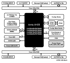
Click to enlarge- Block Diagram


