


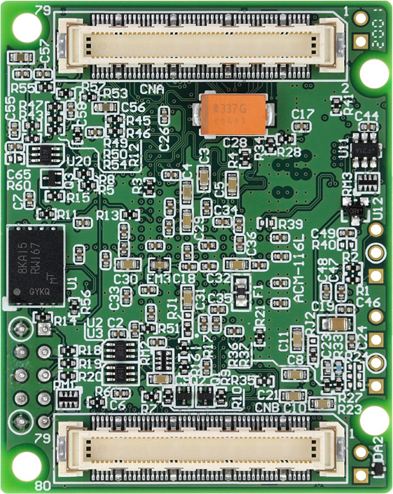
| FPGA overview | XC7A35T | XC7A50T | XC7A75T | XC7A100T | XC7A200T |
|---|---|---|---|---|---|
| Logic Cell | 33,280 | 52,160 | 75,520 | 101,440 | 215,360 |
| Slice | 5,200 | 8,150 | 11,800 | 15,850 | 33,650 |
| Max Distributed RAM (kb) | 400 | 600 | 892 | 1,188 | 2,888 |
| Max Block RAM (kb) | 1,800 | 2,700 | 3,780 | 4,860 | 13,140 |
| DSP Slice | 90 | 120 | 180 | 240 | 740 |
| CMT (MMCMx1 + PLLx1) | Five | Five | 6 | 6 | Ten |
| GTP Channel (Device) | Four | Four | Four | Four | Four |
| GTP Channel ( Board ) | 2 | 2 | 2 | 2 | 2 |
| Max user I / O (Device) | 250 | 250 | 250 | 285 | 285 |
| Max user I / O ( Board ) | 128 | 128 | 128 | 128 | 128 |
For details on the FPGA overview, see the XILINX Artix-7 page .
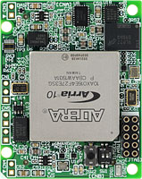
■ Equipped with XC7A35T-1FGG484C, XC7A50T-1FGG484C,
XC7A75T-1FGG484C, XC7A100T-1FGG484C,
or XC7A200T-1FBG484C
■ Abundant I / O extraction (128)
CNA: 64 (High Range) Vcco = 3.3V
CNB: 64 (High Range) Vcco = External input
■ Onboard clock
General purpose: 50MHz (LVTTL)
External input possible (CNA / CNB)
■ RocketIO Evaluable
TX / RX 2ch each
Reference clock: 125MHz (LVDS), External input possible (MMCX) )
125 / 150MHz and communication standard
■ Configuration ROM
Quad SPI ROM: N25Q064 / 128 (Micron, 64Mbit / 128Mbit)
ISP possible from iMPACT
■ DDR3 SDRAM installed
Micron: MT41J64M16 (1Gbit)
■ 7-pin JTAG connector installed
FPGA configuration
Configuration ROM ISP
JTAG Buffer circuit Achieves stable download
■ 3.3V single power supply operation
1.0V, 1.2V, 1.5V, 1.8V, 2.5V generated in board
Power sequencer installed (when turned on )
■ General-purpose LED x2
■ General-purpose switch x2
Push button switch x1
DIP switch x1bit
■ Reset function for configuration
■ Separate Vcco (CNB) (Tested at 3.3V at the time of manufacture)
■8-layer board adopted
■ I / O wiring length control (memory is managed separately)
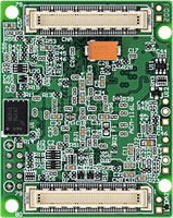
■ Half card size 54mm x 43mm ■ RoHS directive compliant
CNA CNB A board IOA0-63
MAX 40.4mm
MIN 20.5mmIOB0-63
MAX 30.9mm
MIN 12.3mm
- Not all I / O is LVDS compatible
- Users are requested to consider each I / O standard based on FPGA materials.
 Click to enlarge |
Click the block diagram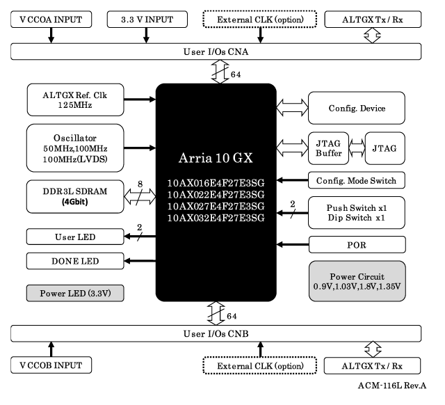 to enlarge |
 |


