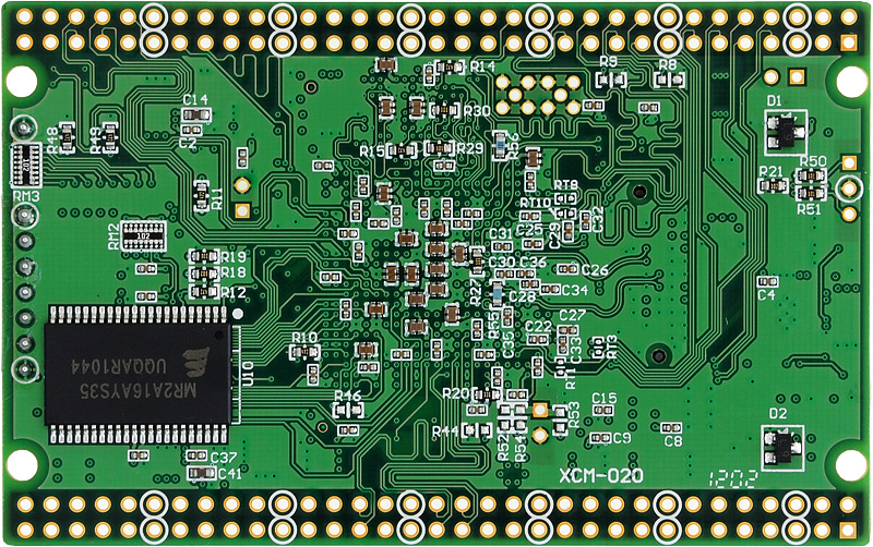
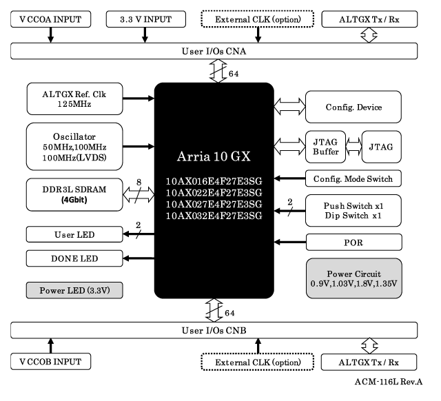
| FPGA function overview |
| Features of the Cyclone IV E FPGA device family |
| Item | EP4CE30 | EP4CE40 | EP4CE115 |
| Logic Elements | 28,848 | 39,600 | 114,480 |
| Embedded memory (Kbits) | 594 | 1,134 | 3,888 |
| Embedded 18 x 18 multipliers | 66 | 116 | 266 |
| General-purpose PLLs | Four | Four | Four |
| Global Clock Networks | 20 | 20 | 20 |
| Maximum user I / O pins (Device) | 532 | 532 | 528 |
| Maximum user I / O pins ( Board ) | 296 | 296 | 296 |
For more information on FPGA overview, see the page of ALTERA Cyclone IV .
■ Equipped with EP4CE30F29C8N, EP4CE40F29C8N or EP4CE115F29C8N
■ Equipped with DDR2-SDRAM
MT47H64M16HR, (Micron, 1Gbit)
2Gb can also be installed, (Custom order)
■ Equipped with serial FLASH-ROM
M25P16 (Micron, 16Mbit)
■ Equipped with configuration ROM
EPCS Altera: 64Mbit)
■ 50MHz with onboard clock , external input possible ■ 8 general-purpose LEDs ■
3 general-purpose switches
Push button switch x2
DIP switch x1 bit
■ 296 I / O pins pulled out externally
■ JTAG connector
download
Achieves safe and stable access with a 10-pin socket
JTAG buffer that supports various cables such as USB Blaster
■ 2 status LEDs
CONF_DONE, POWER
■ Equipped with a reset circuit for configuration
■ 3.3V single power supply operation
Generates 2.5V, 1.8V, 1.2V in the board
■ VCCIO can be separated (tested at 3.3V at the time of manufacturing)
■ 8-layer board adopted
■ I / O wiring length control
| Product | connector | CNA | CNB | CNC | CND | Remarks |
|---|
| Common | Wiring length (Min) | 33mm | 24mm | 32mm | 22mm | B board |
| Wiring length (Max) | 59mm | 43mm | 52mm | 44mm |
30C8
40C8 | Number of LVDS pairs
(including True-LVDS numbers) | --- | 13
(0) | 8
(8) | 10
(8) |
| 115C8 | Number of LVDS pairs
(including True-LVDS numbers) | --- | 32
(0) | 42
(42) | 42
(20) |
* LVDS is limited to BANK belonging to the connector that can input Vccio
* The receiving terminator cannot be mounted on the board
* For details, see the pin assignment table in the product document.
■ Board dimensions: 54mm x 86mm Credit card size RoHS compliant