function EP1C6Q240C8N EP1C12Q240C8N Logic Elements 5,980 12,060 M4K RAM blocks
(128X26 bits)20 52 Total number of RAM bits 92,160 239,616 Number of PLLs 2 2 Maximum user I / O pins
(Device)185 173 Maximum user I / O pins
( Board )100 100
■ FPGA
EP1C6Q240C8N or EP1C12Q240C8N
■ 100 I / O available
■ 5V compatible level converter (74LVCC3245) mounted
Basically input / output can be switched every 8 bits (FPGA control)
■
Various JTAG connector download cables (USB Blaster) , BL3, ByteBlasterII, ByteBlasterMV, etc.) Compatible 10-pin socket
■ AS mode connector We
plan to abolish the AS mode connector in the future
How to write to EPCS via JTAG by JIC file
PS mode is not supported. ..
■ clock source
30 MHz
■ Configuration ROM
EPCS4 (10000 times or more rewritable)
■ reset circuit
■ Status LED
POWER-LED POWER-ERROR-LED
■
2 general-purpose LEDs
■ Power supply circuit
5V single power supply (built-in 3.3V, 1.5V generation circuit required inside)
■ 6-layer board adopted
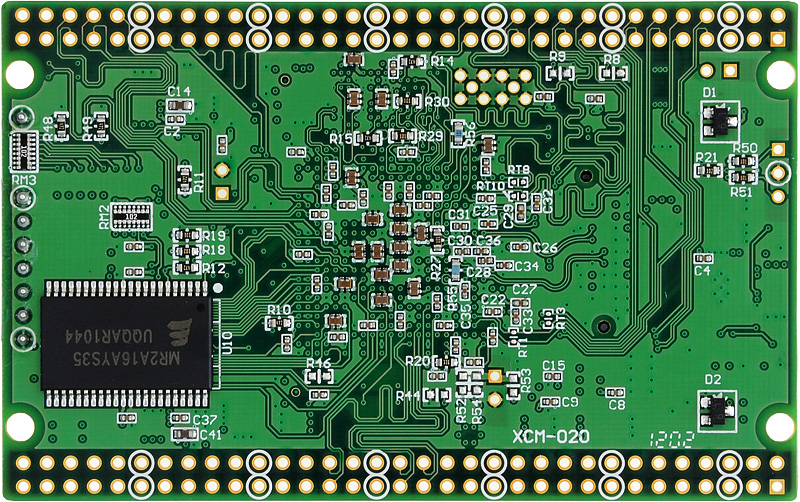
■ Board dimensions: 54mmX86mm Credit card size RoHS directive compliant

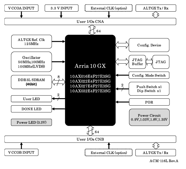
Click to enlargeClick the block diagram to enlarge