| FPGA overview | XC7K160T | XC7K325T | XC7K410T |
|---|---|---|---|
| Logic Cell | 162,240 | 326,080 | 406,720 |
| Slice | 25,350 | 50,950 | 63,550 |
| Max Distributed RAM (kb) | 2,188 | 4,000 | 5,663 |
| Total Block RAM (kb) | 11,700 | 16,020 | 28,620 |
| DSP Slice | 600 | 840 | 1,540 |
| CMT (MMCMx1+PLLx1) | 8 | Ten | Ten |
| Max user I/O (Device) | 400 | 500 | 500 |
| Max user I/O (Board) | 296 (HR 172) (HP 124) | 296 (HR 172) (HP 124) | 296 (HR 172) (HP 124) |
Please refer to the page of XILINX Kintex-7 for details of FPGA outline .
- Equipped with XILINX Kintex-7 XC7K160T-1FBG676C or
XC7K325T-1FBG676C or XC7K410T-1FBG676C - Abundant I/O externally pulled out (296)
- IOA (CNA connector): 64 (HR)
- IOB (CNB connector): 64 (HR)
- IOC (CNC connector): 84 (HR 44, HP 40)
- IOD (CND connector): 84 (HP)
*HR is High Range I/O and supports I/O voltage from 1.2V to 3.3V
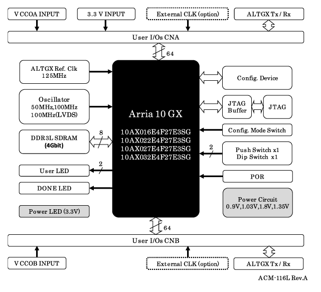
*HP is High Performance I/O supports I/O voltage from 1.2V to 1.8V - On-board clock
- General purpose: 50MHz (Vcco interlocking)
- External input possible (CNA/CNB/CNC/CND)
- Configuration ROM
Quad SPI ROM: MT25QL128 (Micron, 128Mbit)
FPGA with 7-pin JTAG connector Configuration
ISP
JTAG Buffer circuit to configuration ROM for stable download- Power supply: 3.3V, VIOLA, VIOLB, VIOLC, VIOLD
VCCINT, 1.0V, 1.8V, 2.0V are generated on the board
Power supply sequencer installed (when turned on ) - General-purpose LED: 2
- General-purpose switch: 2
- Push button switch x1
- DIP switch x1bit
- Reset function for configuration
- Separated Vcco (CNA/CNB/CNC/CND) (tested at 1.8V during production)
- Uses an 8-layer board
- I/O wiring length control
CNA
IOA[0..63]CNB
IOB[0..63]CNC
IOC[0..83]CND
IOD[0..83]A board MAX 36.09mm
MIN 30.18mmMAX 40.85mm
MIN 34.35mmMAX 43.07mm
MIN 35.32mmMAX 38.31mm
MIN 32.84mm- For details, please consider based on the FPGA material and board circuit diagram.
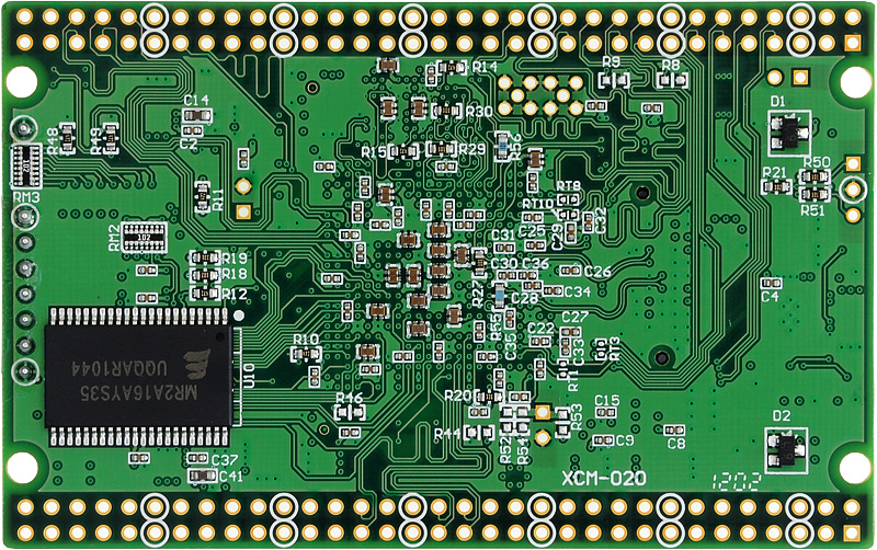
- Board size: 54mm x 86mm Credit card size
- RoHS compliant
- Block Diagram
 RoHS compliant